Vincent D'Onofrio Weighs In On Daredevil: Born Again's Reset

A new Monarch: Legacy of Monsters poster has double the Russells. Get a look at the Go Go! Loser Ranger anime adaptation. Disney+’s new Goosebumps show drops a creepy new clip. Plus, what’s coming on Chucky, Quantum Leap, and more. Spoilers get!

Read more…


Source: Gizmodo – Vincent D’Onofrio Weighs In On Daredevil: Born Again’s Reset

Atlassian To Buy Video Messaging Provider Loom for Nearly $1 Billion

Atlassian said on Thursday it had agreed to acquire privately held video messaging platform Loom for about $975 million, beefing up its team collaboration tools to tap into resilient demand fueled by the adoption of hybrid work. From a report: Integration of Loom’s technology into Atlassian software such as collaboration tools Jira and Confluence will help users use video in their workflows. The acquisition of Loom, which has more than 25 million users globally, will enable customers communicate and collaborate more effectively, Atlassian said.

Read more of this story at Slashdot.


Source: Slashdot – Atlassian To Buy Video Messaging Provider Loom for Nearly Billion

HBM4 in Development, Organizers Eyeing Even Wider 2048-Bit Interface

High-bandwidth memory has been around for about a decade, and throughout its its continued development it has steadily increased in speed, starting at a data transfer rate from 1 GT/s (the original HBM) and reaching upwards of 9 GT/s with the forthcoming HBM3E. This has made for an impressive jump in bandwidth in less than 10 years, making HBM an important cornerstone for whole new classes of HPC accelerators that have since hit the market. But it’s also a pace that’s getting harder to sustain as memory transfer rates increase, especially as the underlying physics of DRAM cells have not changed. As a result, for HBM4 the major memory manufacturers behind the spec are planning on making a more substantial change to the high-bandwidth memory technology, starting with an even wider 2048-bit memory interface.


Designed as a wide-but-slow memory technology with an ultra-wide interface running at a relatively modest clockspeed, HBM’s current 1024-bit memory interface has been a defining characteristic of the technology. Meanwhile its modest clockspeeds have become increasingly less modest in order to keep improving memory bandwidth. This has worked thus far, but as clockspeeds increase, the highly parallel memory is risking running into the same signal integrity and energy efficiency issues that challenge GDDR and other highly serial memory technologies.


Consequently, for the next generation of the technology, organizers are looking at going wider once more, expanding the width of the HBM memory interface even further to 2048-bits. And, equally as important for multiple technical reasons, they intend to do this without increasing the footprint of HBM memory stacks, essentially doubling the interconnection density for the next-generation HBM memory. The net result would be a memory technology with an even wider memory bus than HBM today, giving memory and device vendors room to further improve bandwidth without further increasing clock speeds.


As planned, this would make HBM4 a major technical leap forward on multiple levels. On the DRAM stacking side of matters, a 2048-bit memory interface is going to require a significant increase in the number of through-silicon vias routed through a memory stack. Meanwhile the external chip interface will require shrinking the bump pitch to well below 55 um, all the while increasing the total number of micro bumps significantly from the current count of (around) 3982 bumps for HBM3.


Adding some additional complexity to the technology, memory makers have indicated that they are also going to stack up to 16 memory dies in one module; so-called 16-Hi stacking. (HBM3 technically supports 16-Hi stacks as well, but so far no manufacturer is actually using it) This will allow memory vendors to significantly increase the capacity of their HBM stacks, but it brings new complexity in wiring up an even larger number of DRAM dies without fault, and then keeping the resulting HBM stack suitably and consistently short.


All of this, in turn will require even closer collaboration between chip makers, memory makers, and chip packaging firms in order to make everything come together smoothly.


Speaking at TSMC’s OIP 2023 conference in Amsterdam, Dan Kochpatcharin, TSMC’s Head of Design Infrastructure Management had this to say: “Because instead of doubling the speed, they doubled the [interface] pins [with HBM4]. That is why we are pushing to make sure that we work with all three partners to qualify their HBM4 [with our advanced packaging methods] and also make sure that either RDL or interposer or whatever in between can support the layout and the speed [of HBM4]. So, [we work with] Samsung, SK Hynix, and Micron.”


Since system-in-package (SiP) designs are getting larger, and the number of HBM stacks supported by advanced chip packages is increasing (e.g. 6x reticle size interposers and chips with 12 HBM stacks on-package), chip packages are getting more complex. To ensure that everything continues to work together, TSMC is pushing chip and memory designers to embrace Design Technology Co-Optimization (DTCO). This being a big part of the reason why the world’s largest foundry recently organized 3DFabric Memory Alliance, a program designed to enable close collaboration between DRAM makers and TSMC in a bid to enable next-generation solutions that will pack huge amounts of logic transistors and advanced memory.


Among other things, TSMC’s 3DFabric Memory Alliance is currently working on ensuring that HBM3E/HBM3 Gen2 memory works with CoWoS packaging, 12-Hi HBM3/HBM3E packages are compatible with advanced packages, UCIe for HBM PHY, and buffer-less HBM (a technology spearheaded by Samsung).


Overall, TSMC’s comments last week give us our best look yet at the next generation of high-bandwidth memory. Still, additional technical details about HBM4 remain rather scarce for the moment. Micron said earlier this year that ‘HBMNext’ memory set to arrive around 2026 will offer capacities between 36 GB and 64 GB per stack and peak bandwidth of 2 TB/s per stack or higher. All of which indicates that memory makers won’t be backing off on memory interface clockspeeds for HBM4, even with the move to a wider memory bus.


Source: AnandTech – HBM4 in Development, Organizers Eyeing Even Wider 2048-Bit Interface

Threads Will Not Amplify News on The Platform, Says Instagram's Mosseri

Head of Instagram Adam Mosseri said Wednesday that Threads will not amplify news on the platform. Users are flocking to Threads for up-to-date information about the Israel-Hamas conflict, the Ukraine war, and the 2024 election, but the platform will not be making the content any easier to find.

Read more…


Source: Gizmodo – Threads Will Not Amplify News on The Platform, Says Instagram’s Mosseri

Unemployed Hideki Kamiya, the Guy Who Spearheaded Bayonetta, Is Now a YouTuber

On Hideki Kamiya’s first video for his new YouTube channel, the man who helped direct landmark games like Bayonetta, Okami, Viewtiful Joe, and Devil May Cry is seen walking out of Platinum Games’ headquarters carrying the trademark cardboard box of the recently laid off. He’s wearing shorts and an orange bandana.

Read more…


Source: Gizmodo – Unemployed Hideki Kamiya, the Guy Who Spearheaded Bayonetta, Is Now a YouTuber

AMD Moves to Acquire Nod.ai to Build Out AMD’s AI Solution

Every chip vendor is in a race to provide the best hardware to compete in the massively accelerating AI market. While hype may be a bit ahead of reality now regarding AI capabilities, the speed of AI advancement is closing that gap surprisingly rapidly. Chip vendors like AMD, Intel, Qualcomm and the current AI market leader, NVIDIA, are moving very rapidly to understand and embrace this opportunity.

What is quickly becoming evident is that just focusing on the hardware isn’t good enough. These vendors must also develop AI software competence which was demonstrated early on with NVIDIA’s massive two-decades-long effort to bring AI to the market at scale. Intel is significantly increasing its own software capabilities, and AMD, not wanting to be left behind, has been ramping up, as well.  

AMD’s recent move to acquire Nod.ai is a case in point and should significantly and very rapidly advance AMD’s AI capabilities.

Let me explain. 

NPUs and GPUs + Software

AMD is one of several vendors that will have a complete hardware set for AI shortly, including low-performance, highly efficient NPUs (Neural Processing Units) and high-performance, less efficient GPU solutions. Used in concert, they should provide the breadth of hardware needed to both run high-performance AI workloads as well as persistent low-performance edge AI workloads where energy efficiency is more important. 

To do this effectively, they will need to both understand the AI engines intimately and better understand the AI software that will run on it, otherwise the solutions are likely to underperform hardware vendors who have developed a stronger AI software proficiency and are better able to tune their products to meet related demand.  

If AMD doesn’t understand deeply the AI solutions and can’t provide the necessary performance advantages, the AI market will pass it by. But AMD isn’t a company that intends to let that happen, so it acquired the AI software-enabling company, Nod.ai.  

This fits with AMD’s award-winning CEO Lisa Su’s IBM training. One of IBM’s historic advantages is co-developing hardware and software together. It’s still arguably the market leader in mature tested AI technology with its watson.x solution.  

Nod.ai

Nod.ai creates enabling software for future AI deployments. In other words, it makes AI run better, but doesn’t generally compete with AI vendors like OpenAI, allowing it to move between AI providers to create solutions that significantly enhance the performance of third-party AIs in a way that shouldn’t upset the AI providers.  

Tying Nod.ai to AMD makes a lot of competitive sense. If an AI can be made to run better on a vendor’s hardware, those that buy that AI are likely to favor the hardware it runs best on, and Nod.ai will assure that AI software runs best on AMD.

This should provide a strong competitive advantage to AMD once the company is acquired and merged because not only will AMD have unparalleled access to Nod.ai’s tools, but the two companies will then work harder together to create a unique and powerful solution.

In addition, Nod.ai has been favoring AMD for some time in its solutions, suggesting that this greater integration resulting from the merger already exists due to Nod.ai seeming to favor AMD, providing a far faster path to market with a related AMD/Nod.ai blended solution.  

In short, the two companies already seem to be working together well, suggesting the benefits to AMD for this merger should emerge unusually rapidly. 

Wrapping Up:

Vendors like AMD are rapidly adjusting to the AI opportunity, but those with enhancing software will likely have the strongest market advantage. Anticipating this, AMD has moved to acquire Nod.ai, an AI enabling software company that has the potential to give AMD a significant advantage in creating and providing advanced AI solutions. 

This acquisition again shows that AMD is here to play and plans to aggressively go after and seize this new AI opportunity and make it theirs. 


Source: TG Daily – AMD Moves to Acquire Nod.ai to Build Out AMD’s AI Solution

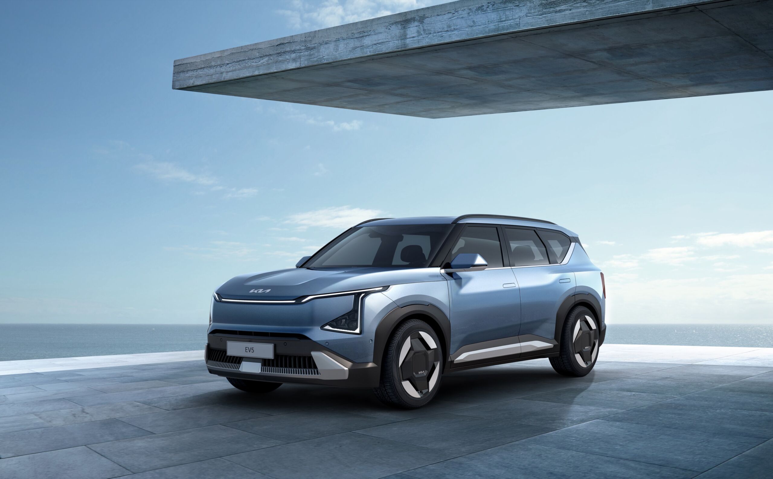
Kia debuts the EV5 SUV alongside two new affordable electric concepts

At Kia’s EV day event, the automaker has launched its upcoming electric vehicle, the EV5, and introduced two new concepts meant to make the technology more accessible. The company says it aims to offer people a wide-ranging EV lineup that includes the EV6 and the newer EV9, which promises Level 3 autonomy and a 336-mile range. It’s hoping to sell the EV5 and, eventually, the EV4 and EV3 at prices ranging from $35,000 to $50,000 “to accelerate the widespread adoption of EVs.”

The EV5 SUV is the third purely electric vehicle in its lineup. Kia designed it on top of E-GMP, its dedicated EV platform, and currently plans to manufacture and sell them in China and Korea. Its specifications differ for each market, with China getting a standard, a long-range and a long-range AWD variant. China’s standard model will come with a 64kWh battery pack, along with a 160kW motor, and is expected to have a range of 530 km or 329 miles. 

Meanwhile, the long-range version will have a bigger battery that can reach a range of 720 km or 447 miles on a single charge. The AWD model will have a range of 650 km or 404 miles and will come with a fast-charging capability. As for the Korean models, their range will apparently be tailored to meet market demands. Kia says a GT variant with performance features will also be unveiled at a later date. 

A small SUV
Kia

While the EV5 is very much a real product that will initially be available for sale in the Chinese market later this year, the other electric vehicles Kia unveiled during its event are still a concept at this point. The EV3 (pictured above), if it turns out exactly as the automaker has envisioned, will be a compact and accessible version of the EV9. Kia’s EV4 (below), on the other hand, will be a sedan with a low nose, sharp lines and a futuristic cocoon-like interior. It remains to be seen whether Kia can achieve a $35,000 price point, which seems to be a common target among EV makers, for any of the aforementioned vehicles.

A Chrome sedan.
Kia

This article originally appeared on Engadget at https://www.engadget.com/kia-debuts-the-ev5-suv-alongside-two-new-affordable-electric-concepts-122040979.html?src=rss

Source: Engadget – Kia debuts the EV5 SUV alongside two new affordable electric concepts

TSMC: Importance of Open Innovation Platform Is Growing, Collaboration Needed for Next-Gen Chips

This year TSMC is commemorating 15 years of its Open Innovation Platform, a multi-faceted program that brings together the foundry’s suppliers, partners, and customers to help TSMC’s customers better build innovative chips in an efficient and timely manner. The OIP program has grown over the years and now involves tens of companies and over 70,000 IP solutions for a variety of applications. It continues to grow, and its importance will get higher than ever when next generation technologies, such as 2 nm, and advanced packaging methods become mainstream in the coming years.


“This is not a marketing program, it is actually an engineering program to enable the industry,” said Dan Kochpatcharin, Head of Design Infrastructure Management at TSMC, at the OIP 2023 conference in Amsterdam, the Netherlands. “We have a huge engineering team behind to work with the EDA partners, IP partners, and design partners.”


Shrinking Time-to-Market


Speeding up time-to-market is one of the corner stones of TSMC’s OIP program. Before emergence of the OIP program in 2008, TSMC would develop a process technology and process development kits (PDKs) in about 18 months time, then hand over PDKs and design rules to its partners among electronic design automation (EDA) software and IP developers. The latter would spend another 12 months creating EDA tools and building IP blocks before supplying programs and IP solutions to actual chip designers. Then it would take chip developers another 12 months to build actual chips. 


With OIP, TSMC’s  EDA tool and IP design partners can start development of their products a few months after TSMC begins development of its new production node. And, by the time TSMC finalizes its process technology, EDA tools and IP are ready for chip designers, the foundry claims. This speeds up time-to-market by about 15 months, TSMC says. Meanwhile, as development time for new nodes is stretching and so is development time for chips, the value of early collaboration between TSMC and EDA and IP providers is increasing. 


For example, TSMC has been working with its partners on N2 (2nm-class) EDA and IP readiness for two years now, with TSMC aiming to have tools and common IP ready for chip designers in H2 2025. 


Quality Matters


An avid reader would wonder why, even with the success of the program, OIP only grew to 39 IP members in 15 years. As it turns out, TSMC is extremely picky with companies that join the program, according to Dan Kochpatcharin. TSMC needs members of the OIP program to really contribute to it and make the joint effort something bigger than the sum of all parts. Because TSMC clients use IP, software, and services offered by participants of the OIP program, the latter have to be really good in their fields to be a part of OIP.


In fact, TSMC even has its TSMC9000 program (the name mimics ISO 9000 quality policy) that sets quality requirements for IP designs. IP collaborators undergo TSMC9000 evaluations, with results available on TSMC-Online, guiding customers on IP reliability and risks. 


“We do a lot of qualifications for IP, before the test shuttles they do tape outs, and then they have TSMC 9000 checklists, […] customer can see [all] the results on TSMC-Online,” explained Kochpatcharin. “So, they can see okay, this IP got silicon introductions, so, they have more confidence in the IP. [They also see] how many customers adopted [this IP], how many tape outs, and how many productions. For the lack of a better term, Consumer Report for IP.”


Alliance members list their IPs in TSMC’s premier catalog, which features thousands of IP options from 39 contributors. Customers can search for IPs using the ‘IP Center’ on the TSMC-Online Design Portal. Each IP in the catalog is developed, sold, and supported by its originating partner. Meanwhile, chip developers can even check out how popular is one IP or another, which can give chip developers some more confidence in their choice. Confidence is something important today and will be even more important for 3 nm, 2 nm, and future nodes as tape outs get more expensive.


Six Alliances


But speeding up time-to-market and ensuring quality are not the only purposes of the OIP program. It is meant to simplify development, production, testing, and packaging of chips. TSMC’s OIP involves a variety of members and is organized into six programs or alliances, each responsible for a separate line of work: 


  • IP Alliance that that is focused on providing silicon-verified, production-proven and foundry-specific intellectual property (IP) that TSMC customers can choose from.
  • EDA Alliance that includes companies which offer electronic design automation (EDA) software that is compliant with TSMC technology requirements and support the foundry’s production nodes.
  • Design Center Alliance which comprises of contract chip designers as well as companies offering system level design solution enablement.
  • Cloud Alliance that combines EDA toolmakers and cloud service providers enabling TSMC’s customers to develop and simulate their chips in the cloud to reduce in-house compute needs.
  • 3D Fabric Alliance that unites all companies responsible for advanced packaging as well as development of multi-chiplet processors, which essentially includes all of the abovementioned companies as well as makers of memory (including Micron, Samsung, and SK Hynix), substrates, OSATs, and makers of test equipment.
  • Value Chain Alliance that resembles Design Center Alliance, but is meant to offer a broader range of contract chip design services and IP offerings to cater to needs of a broad range of customers spanning from startups and OEMs to ASIC designers. 


The 3D Fabric Alliance program was introduced late last year, so it can be considered the newest addition to OIP. Meanwhile, 3DFabric Alliance looks to be expanding fast with new members and for a reason.


Multi-Chiplet Designs Become New Standard


Process technologies are getting more complex, and this is not going to change. Chip design workflow might get a little easier going forward as EDA makers like Ansys, Cadence, Siemens EDA, and Synopsys are incorporating artificial intelligence capabilities into their tools. But because High-NA EUV lithography scanners halve reticle size from 858 mm2to 429 mm2, it looks like the majority of AI and high-performance computing (HPC) processors are going to adopt multi-tile design in the coming years, which will drive the need for software that assists creation of multi-tile solutions, advanced packaging, HBM-type memory, and all-new methods of testing. This will again increase importance of industry-wide collaboration and the importance of TSMC’s OIP.


“[We have offered InFO_PoP] and InFO_oS 3D IC since 2016, [3D ICs have been] in production for years already, [but] back then it was still a niche [market],” said Kochpatcharin. “The customer had to know what they were doing […] and only a few people could do a 3D IC [back then]. [In] 2021 we launched the 3DFabric activity, we wanted to make it generic for everybody because with AI and HPC coming [from multiple companies], [these] cannot be niche things anymore. So, everybody has to be able to use 3D IC. [For example], automotive is a wonderful [application for] 3D IC, there is a [huge] market out there.”


Meanwhile, to enable next-generation connectivity between chips and between chiplets, TSMC envisions silicon photonics will be needed, so the company is actively working in this direction within its OIP program. 


“If you go to N2 and the next one coming up is silicon photonics,” said Kochpatcharin. “This is where we launched a process needed to have [design service partners] to be able to support the customer.”


Source: AnandTech – TSMC: Importance of Open Innovation Platform Is Growing, Collaboration Needed for Next-Gen Chips

SAG-AFTRA accuses studios of 'bully tactics' after talks break down

Two weeks have passed since the Writers Guild of America reached a deal to resume working, but things aren’t looking good for its counterpart, the Screen Actors Guild-American Federation of Television and Radio Artists (SAG-AFTRA). Talks broke down Wednesday night with the Alliance of Motion Picture and Television Producers (AMPTP) due to “bully tactics,” with CEOs reportedly walking away without any proposed counteroffer, SAG-AFTRA’s negotiating committee said in a statement. CEOs such as Disney’s Bob Iger and Netflix’s Ted Sarandos started personally meeting with SAG-AFTRA negotiators in early October. 

The committee is working to reach an agreement for actors, striking since mid-July. “We have negotiated with them in good faith, despite the fact that last week they presented an offer that was, shockingly, worth less than they proposed before the strike began,” SAG-AFTRA added. “These companies refuse to protect performers from being replaced by AI, they refuse to increase your wages to keep up with inflation, and they refuse to share a tiny portion of the immense revenue your work generates for them.”

The AMPTP claims a requested cut in streaming revenue would cost $800 million a year, a figure SAG-AFTRA says is inflated by 60 percent after “big, meaningful counters” from the union. According to SAG-AFTRA, this tactic is an attempt to fool members and break down support. The union also claims AMPTP is requiring day one AI consent from actors to use their likeness across an entire franchise. For now, SAG-AFTRA encourages its members to continue showing up at picket lines and solidarity events. 

This article originally appeared on Engadget at https://www.engadget.com/sag-aftra-accuses-studios-of-bully-tactics-after-talks-break-down-114617412.html?src=rss

Source: Engadget – SAG-AFTRA accuses studios of ‘bully tactics’ after talks break down

Woman's Experimental Bionic Hand Passes Major Test With Flying Colors

Scientists appear to have developed a hand prosthetic that provides much more control and comfort than those available today. In new research this week, they’ve detailed the case of a Swedish woman who has successfully worn the advanced bionic limb for years with no major issues, while experiencing significantly less…

Read more…


Source: Gizmodo – Woman’s Experimental Bionic Hand Passes Major Test With Flying Colors

The Morning After: Our verdict on Google’s Pixel 8 Pro

The reviews keep coming this week. After all the AI tricks, rock-climbing and specification barrage we saw at Google’s big Pixel reveal event, how do Google’s flagship smartphones stack up?

Pretty well, according to our reviews of both the Pixel 8 Pro and Pixel 8. The surprise highlight is AI, using machine learning and its homemade Tensor G3 chip in a tangible and practical way compared to services like ChatGPT or Midjourney. This includes making your photos look better, videos sound better and adds interactive robo-voice panache to call screening.

TMA
Engadget

Both devices once again have incredibly capable cameras, with 5x optical zoom on the Pixel 8 Pro (matching the iPhone 15 Pro Max) and new pro controls too. According to Engadget’s Sam Rutherford, the Pixel 8 Pro feels like the most powerful smartphone camera on the market.

If there is one caveat, both the Pixel 8 and 8 Pro cost $100 more than their predecessors. In the review, we break down all the new AI features and test the cameras out at that classic photo event — a coworker’s wedding.

(We also reviewed the Pixel Watch 2, but it’s less of a ringing endorsement.)

— Mat Smith

​​You can get these reports delivered daily direct to your inbox. Subscribe right here!​​

The biggest stories you might have missed

The Zwift Hub One trainer offers virtual shifting and broader bike compatibility

Google brings back smart speaker grouping after Sonos lawsuit victory

How to watch the ring of fire solar eclipse on October 14

Pixel Watch 2 review: Not leading the way, but no longer lagging

The FTC wants to ban hidden ‘junk fees’ that jack up the price of your purchases

Crunchyroll will pay you $30 for violating your data privacy rights

California’s right to repair bill is now California’s right to repair law

Governor Newsom signed the legislation Tuesday.

TMA
Phone-Service-Centre via Getty Images

California is the third state to pass a right to repair consumer protection law, following Minnesota and New York. The California Right to Repair bill was originally introduced in 2019.

“This is a victory for consumers and the planet, and it just makes sense,” Jenn Engstrom, state director of CALPIRG, told iFixit. “Right now, we mine the planet’s precious minerals, use them to make amazing phones and other electronics, ship these products across the world and then toss them away after just a few years’ use.”

There are exceptions to the rules. No, it doesn’t cover your PS5 — not even that new skinny one. Nor are alarm systems or heavy industrial equipment that “vitally affects the general economy of the state, the public interest and the public welfare.”

Continue reading.

EU official gives Mark Zuckerberg 24 hours to respond to Israel misinformation concerns

It comes a day after a similar letter to X owner Elon Musk.

The European Union’s regulatory commissioner posted a single-page correspondence to Meta CEO Mark Zuckerberg, giving the Facebook founder 24 hours to respond. The letter acknowledges areas where Meta’s content moderation has improved but raises concerns about misinformation (including deepfakes) on the company’s social platforms as the Israel–Hamas conflict continues.

The EU’s Digital Services Act (DSA) requires social companies, like Meta, to moderate and remove illegal and harmful content. The law requires platforms operating in the EU to police malicious material proactively. It can levy fines of up to six percent of any infringing companies’ total revenue.

Continue reading.

NASA reveals what it found on the asteroid Bennu

The OSIRIS-REx even returned ‘bonus asteroid material.’

TMA
NASA

In a livestream show-and-tell, NASA scientists outlined what they’ve discovered so far. The big news here is that samples from the 4.5-billion-year-old Bennu asteroid contain not only carbon, but also water. These are the building blocks of life on Earth and, likely, everywhere else. These samples have only been on the planet since September 25, and initial studies just began. NASA also noted it got “bonus asteroid material” covering the outside of the collector head, canister lid and base.

Continue reading.

Microsoft might owe $28.9 billion in back taxes

It needs to check its spreadsheets again.

Microsoft owes the Internal Revenue Service (IRS) $28.9 billion in back taxes, not including penalties and interest, at least according to the tax authority. The tech giant has revealed in a filing with the Securities and Exchange Commission that it received a series of Notices of Proposed Adjustment (NOPAs) from the IRS for the tax years 2004 to 2013. Microsoft has been working with the IRS for nearly a decade to address the questions about how it distributed its profits among countries and jurisdictions. The result is this multi-billion-dollar tax bill. The company disagrees, as expected, and said newer tax laws could reduce the back taxes it owes from this particular audit by $10 billion. That’s still $18.9 billion, though.

Continue reading.

This article originally appeared on Engadget at https://www.engadget.com/the-morning-after-our-verdict-on-googles-pixel-8-pro-111554730.html?src=rss

Source: Engadget – The Morning After: Our verdict on Google’s Pixel 8 Pro

X CEO responds to EU officials over handling of Israel-Hamas disinformation

Linda Yaccarino, X’s CEO, says the company has redistributed its resources and has refocused internal teams, which are now working round the clock to address the platform’s needs related to the ongoing Israel-Hamas war. Yaccarino talked about the measures the website has taken so far to contain fake news about the Hamas attacks on Israel, along with hateful posts in support of terrorism and violence, in her response to EU officials. 

On October 10, EU Commissioner Thierry Breton sent Elon Musk an “urgent letter,” calling his attention and reminding him of X’s content moderation obligations under the region’s Digital Services Act. Breton said the EU had indications that the platform formerly known as Twitter is being used to disseminate illegal content and disinformation. Some of the images being circulated on the website, Breton said, were manipulated images from unrelated armed conflicts. Others, including supposed footage of military action, were taken from video games. 

Indeed, Open Source Intelligence (OSINT) researchers told Wired that they’d been inundated with false information on the website, making it difficult to rely on X for information gathering. In the past, posts from news outlets on the ground and reputable sources quickly showed up on people’s timelines. But now, the website’s algorithm is boosting posts by users paying $8 a month for their blue checkmarks, even if they’re misleading content and lies. It didn’t help that Musk himself endorsed two accounts that had previously been proven to post false information to those who want to follow details about the war. One of those accounts also openly post antisemitic comments. 

In her response, Yaccarino claimed that X has removed or labeled “tens of thousands of pieces of content” since the attack on Israel began. She also said that X has deleted hundreds of Hamas-affiliated accounts from the platform so far, and that it continues to work with counter-terrorism organizations to prevent further distribution of terrorist content on the website. 

According to Yaccarino, the platform now has over 700 Community Notes, the website’s crowd-sourced fact-checking tool, related to the attack. And since even media posts can now get notes, around 5,000 posts containing images and videos have been marked with the crowd-sourced messages. The CEO said that notes appear for media and image posts within minutes of them being created and for text posts within a median time of five hours, but X is working to make them show up on posts more quickly. 

In his letter, Breton said that the EU received reports from qualified sources that there were “potentially illegal content” circulating on X despite flags from relevant authorities. Yaccarino addressed that directly in her response, writing that the website has not received any notice from Europol and urging the European Commission to provide more details so that it can investigate further. 

This article originally appeared on Engadget at https://www.engadget.com/x-ceo-responds-to-eu-officials-over-handling-of-israel-hamas-disinformation-103956726.html?src=rss

Source: Engadget – X CEO responds to EU officials over handling of Israel-Hamas disinformation

YouTube Passes Netflix As Top Video Source For Teens

A new survey from investment bank Piper Sandler found that teens in the U.S. consume more videos on YouTube than Netflix. CNBC reports: Teens polled by the bank said they spent 29.1% of their daily video consumption time on Google-owned YouTube, beating out Netflix for the first time at 28.7%. Time on YouTube rose since the spring, adding nearly a percentage point, while Netflix fell more than two percentage points. The data point shows that the streaming business is getting more competitive, and highlights YouTube’s strong position as a free provider of online video, especially among young people. “We wonder if this is a push or a pull in regards to the changing consumption habits, as content on YouTube appears to be improving over time and the streaming industry becomes more and more competitive,” Piper Sandler analysts wrote.

Read more of this story at Slashdot.


Source: Slashdot – YouTube Passes Netflix As Top Video Source For Teens

New York lawmakers are cracking down on kids' exposure to social media algorithms

A new bill out of New York is targeting the thing we all have a love-hate relationship with on social media: the algorithm. Governor Kathy Hochul joined lawmakers in introducing the Stop Addictive Feeds Exploitation (SAFE) for Kids Act, which would require a parent or guardian’s consent to access algorithm-based feeds on platforms such as TikTok, YouTube and Instagram. In her statement of support, Hochul called for adults to protect their children and villainized algorithms as technology that “follows” and “preys” on young people.

Lawmakers pointed to a range of studies demonstrating social media’s association with poor mental health and sleep quality in young people — especially with excessive use. “Social media platforms are fueling a national youth mental health crisis that is harming children’s wellbeing and safety,” New York State Attorney General Letitia James said. “Young New Yorkers are struggling with record levels of anxiety and depression, and social media companies that use addictive features to keep minors on their platforms longer are largely to blame. This legislation will help tackle the risks of social media affecting our children and protect their privacy.”

While pages like TikTok’s For You face restrictions, the legislation would allow young people to view content from people they follow without permission. This setup means they can still see accounts with dangerous misinformation or ideals — such as promoting harmful eating habits — as long as they click the follow button. However, the law would also allow parents or guardians to limit the number of hours a person can spend on each app and to restrict access and notifications completely between midnight and 6 AM. Social media platforms that fail to enforce these policies could owe up to $5,000 in damages.

Lawmakers proposed an identical fine for violations of the New York Child Data Protection Act, which was introduced alongside the SAFE for Kids Act. This legislation would ban “collecting, using, sharing or selling” anyone under 18’s personal data unless they receive consent or can prove it absolutely necessary.

SAFE for Kids Act’s sponsors, State Senator Andrew Gounardes and Assemblywoman Nily Rozic, could bring it before the New York legislature as soon as early 2024. The bill has already faced opposition from Meta and TikTok, as well as Tech:NYC, which represents more than 800 tech companies. Concerns range from restricting free speech to losing out on community-building.

The first state-led bill of this kind passed in Utah earlier this year, requiring anyone under the age of 18 to obtain a parent or guardian’s consent to create a social media profile — not just to explore the algorithm. Arkansas enacted a similar law soon after, but a judge blocked it from taking effect in September. Utah’s legislation is set to take effect in early 2024. Each of these cases would require more comprehensive age verification on the part of social media companies, likely reviewing an ID of some sort — not something every early adolescent has.

This article originally appeared on Engadget at https://www.engadget.com/new-york-lawmakers-are-cracking-down-on-kids-exposure-to-social-media-algorithms-095838157.html?src=rss

Source: Engadget – New York lawmakers are cracking down on kids’ exposure to social media algorithms

Logitech launches a Streamlabs plugin for Loupedeck consoles

Logitech is bringing together two acquisitions over the past few years in its quest to provide live streamers the tools they need: The company has just launched a Streamlabs desktop plugin for Loupedeck consoles. If you’ll recall, the company purchased Streamlabs — a popular livestreaming software that offers a robust set of tools for broadcasting on Twitch, YouTube and Facebook — back in 2019. And in July this year, it acquired Loupedeck, which makes video streaming consoles that rival Elgato’s Stream Deck.

The Streamlabs Desktop Plugin 1.0 turns the Loupedeck Live and Live S devices into external controllers for the streaming software. Creators can use the consoles’ dials to control audio more precisely, and they can activate Streamlabs’ desktop commands and view the status of their livestream straight from their Loupedeck device. They can also set up scenes, sources, audio sources and scene collections in Loupedeck’s software, effectively freeing up more space on their monitor, which could instead be used for views of other things, such as their gameplay or chat. Logitech says the new plugin is rolling out with software update 5.8 today and will come preinstalled on all new Loupedeck devices.

“When we acquired Loupedeck earlier this year, we had a goal of providing a more seamless experience for Streamlabs creators from onboarding to everyday use with presets available out of the box for Loupedeck devices,” Ujesh Desai, Logitech G’s general manager said in a statement. “This 1.0 release is our first offering, which accelerates our goal to bring an ecosystem of hardware and software to creators everywhere, enabling them to focus on doing what they do best, which is make amazing content.”

It’s worth noting that Streamlabs and Loupedeck aren’t the only companies Logitech purchased over the past few years as part of its efforts to go all in on streaming. It also purchased Blue Microphones in 2018, and it announced a few months ago that it’s going to start selling Blue’s Yeti mics under the Logitech G branding going forward.

This article originally appeared on Engadget at https://www.engadget.com/logitech-launches-a-streamlabs-plugin-for-loupedeck-consoles-070159158.html?src=rss

Source: Engadget – Logitech launches a Streamlabs plugin for Loupedeck consoles

Kia EV5 revealed, but US future is uncertain for this electric crossover

A rendering of a blue Kia EV5 crossover

Enlarge / There’s a very distinct family resemblance between the EV9 and the EV5 (pictured). (credit: Kia)

Following the launch of the new EV9, the next product in Kia’s EV onslaught is the smaller EV5. And while the first round of EV5s will go on sale in China and South Korea in the coming months, it will still be some time before the compact SUV is offered globally.

Even worse, we aren’t totally sure if the EV5 will come to America; sources within Kia have both confirmed and denied plans to bring this SUV to the US. The company’s president and CEO said it would be headed stateside, but then Kia’s public relations team denied this statement, with other internal sources saying the EV5 would not be offered in the US. Kia confirms that the EV5 will come to North America, but we’re told this just means Canada and possibly Mexico.

Why? It’s complicated. The likely culprit is that the EV5 isn’t planned to be built in North America, making it ineligible for the new Inflation Reduction Act (IRA) tax credit. That $7,500 credit could drastically reduce the price of a new EV, and Kia not being able to make use of this would reduce the EV5’s competitiveness in the US. Just a thought.

Read 9 remaining paragraphs | Comments


Source: Ars Technica – Kia EV5 revealed, but US future is uncertain for this electric crossover

Kia EV3, EV4 concepts look like the future, will soon be a reality

A top-down look at the front half of the Kia EV3 concept

Enlarge / Around the world people are asking for smaller electric vehicles. Someone at Kia has been listening and designed this car, the EV3. (credit: Kia)

Kia is staring down an ambitious goal. The company wants to increase its global electric vehicle sales to 1 million units annually by 2026, further ramping up to 1.6 million by 2030. New products like the EV5 crossover and EV9 SUV will certainly help with this push, but smaller, more affordable EVs will be crucial to Kia’s success, as well. That’s why, despite being called concept cars, the new EV3 and EV4 are thinly veiled glimpses into Kia’s next round of production EVs.

Unveiled at Kia’s EV Day event in South Korea this week, the EV3 and EV4 will arrive in the next few years. The company also spoke about an even smaller EV2 that will be designed for Europe and emerging markets, with the goal for that car being a super-low starting price—something around the equivalent of $30,000.

The EV3 and EV4 ride on the same E-GMP electric vehicle architecture that underpins the Kia EV6 and EV9, as well as sister vehicles like the Hyundai Ioniq 5, Ioniq 6, and Genesis GV60. However, while the current crop of E-GMP vehicles are built with 800 V electrical architecture giving them fast charging speeds, the EV3 and EV4 will use a slightly more cost-effective version of this platform with a 400 V system. That’s a bummer; one of the big highlights of cars like the Kia EV6 is its ability to charge at a max rate of 233 kW. With the EV3 and EV4, we could be looking at a maximum rate of 150 kW—or less.

Read 7 remaining paragraphs | Comments


Source: Ars Technica – Kia EV3, EV4 concepts look like the future, will soon be a reality

Croatia Wants To Turn Superhot Underground Lake Into a 16MW Geothermal Power Plant

A Croatian energy company has discovered an underwater lake of superheated water that meets all the requirements for the construction of a 16MW geothermal power plant. The Next Web reports: The find was the result of a two-year study by state-run power company Bukotermal that sought to find suitable sites for the exploitation of the energy source, generated by heat from the Earth’s core. The research verified the presence of a geothermal water source at Lunjkovec — Kutnjak field, located in the Varazdin County, close to the border with Hungary. The underground lake, located at a depth of 2.4 kilometers, has an average temperature of 142.03 degrees Celsius.

To date, over 2.5 million euros has been invested in the project. However, according to Alen Pozgaj, CEO of Bukotermal, the total cost to build the plant would be around 50 million euros. The news comes just days after the Croatian Ministry of Economy and Sustainable Development awarded five licenses for the exploration of geothermal waters to firms from Croatia, the United Kingdom, and Turkey. […] For now, Bukotermal has a six-month timeframe to propose how it will exploit the newly discovered geothermal pool. The company plans to construct one or more geothermal power plants and heat utilization facilities at the site, with construction expected to start within two years time.

Read more of this story at Slashdot.


Source: Slashdot – Croatia Wants To Turn Superhot Underground Lake Into a 16MW Geothermal Power Plant

Microsoft reveals IRS notice asking for $28.9 billion in back taxes

Microsoft owes the Internal Revenue Service (IRS) $28.9 billion in back taxes, not including penalties and interest, at least according to the tax authority. The tech giant has revealed in a filing with the Securities and Exchange Commission that it received a series of Notices of Proposed Adjustment (NOPAs) from the IRS for the tax years 2004 to 2013. In its filing, it said that it’s been working with the IRS for nearly a decade to address the authority’s questions about how it distributed its profits among countries and jurisdictions, and this is the agency’s decision after a lengthy investigation. 

To be exact, the IRS audit centered around a practice known as “transfer pricing,” which legally allowed companies to allocate profits and expenses between their operations in different regions. Microsoft explained that a lot of large multinational corporations practice this cost-sharing scheme to reflect “the global nature of their business.” In its case, its subsidiaries shared in the costs of developing some IPs, which means that they’re also entitled to the related profits. As AP notes, though, critics of the regulation argue that companies frequently use it to minimize the taxes they have to pay by reporting lower profits in high tax countries, and vice versa. 

Microsoft explained that the issues raised by the IRS are only relevant to those aforementioned years, because it has since changed its corporate structure and practices. Nevertheless, the IRS believes Microsoft owes $28.9 billion in back taxes. The tech giant disagrees, as expected, and said that newer tax laws could reduce the back taxes it owes from this particular audit by $10 billion. Based on its plan of action shared with the SEC, the company intends to contest the decision to the best of its ability: Microsoft said that it will pursue an appeal within the IRS, which typically takes years to complete, and will even “contest any unresolved issues through the courts” if needed. 

This article originally appeared on Engadget at https://www.engadget.com/microsoft-reveals-irs-notice-asking-for-289-billion-in-back-taxes-055326006.html?src=rss

Source: Engadget – Microsoft reveals IRS notice asking for .9 billion in back taxes