Skip to primary content

Prime-WoW

My site, my way, no big company can change this

Prime-WoW

Main menu

  • Home
  • Discord
  • Forums
  • Games
    • 7DtD
      • 7DtD Map
      • 7DtD Official Forums
      • 7DtD Wiki
    • Minecraft
      • Survival Map
      • Vanilla Map
      • FTB Map
      • FTB Wiki
      • Download FTB Client
    • NWN
      • NWN Wiki
      • NWN Lexicon
      • NWN Vault
      • NWNX
      • NWN Info
      • Rhun Guide
    • Terraria
      • Terraria Map
    • WoW
      • Prime-WoW Site
      • WoW Armory
  • Unfiltered RSS
    • Bikes
    • Games
      • Kotaku
      • PS4 News
      • VR
    • Nature
      • TreeHugger
      • Survival
    • Technology
      • Hardware
        • Hot Hardware
      • Linux
        • Linux Today
        • LWN.net
        • LXer
        • Phoronix
        • RPi
      • LifeHacker
      • Akihabara News
      • AnandTech
      • Ars Technica
      • Engadget
      • Gear & Gadgets
      • Geekologie
      • Gizmodo
      • [H]ardOCP
      • io9
      • Slashdot
      • TG Daily

Post navigation

← Previous Next →

IBM creates the world’s first 2 nm chip

Posted on May 7, 2021 by Xordac Prime
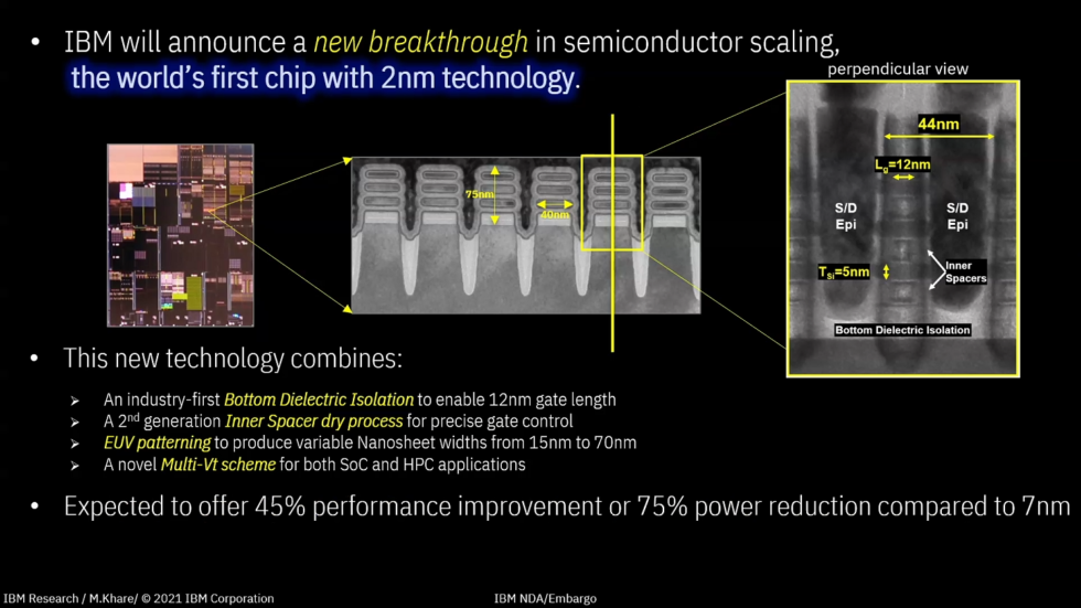
  • This slide from IBM’s preview announcement gives more detail on the new process design. [credit:
    IBM ]

Thursday, IBM announced a breakthrough in integrated circuit design—the world’s first 2 nanometer process. IBM says its new process can produce CPUs capable of either 45 percent higher performance, or 75 percent lower energy use than modern 7 nm designs.

If you’ve followed recent processor news, you’re likely aware that Intel’s current desktop processors are still laboring along at 14 nm, while the company struggles to complete a migration downward to 10 nm—and that its rivals are on much smaller processes, with the smallest production chips being Apple’s new M1 processors at 5 nm. What’s less clear is exactly what that means in the first place.

Originally, process size referred to the literal two-dimensional size of a transistor on the wafer itself—but modern 3D chip fabrication processes have made a hash of that. Foundries still refer to a process size in nanometers, but it’s a “2D equivalent metric” only loosely coupled to reality, and its true meaning varies from one fabricator to the next.

Read 4 remaining paragraphs | Comments


Source: Ars Technica – IBM creates the world’s first 2 nm chip

This entry was posted in Ars Technica, Unfiltered RSS and tagged Ars Technica by Xordac Prime. Bookmark the permalink.
Proudly powered by WordPress